Technology
CMOS optimized for iteration.
xSilica deliberately operates at micron-scale geometries.
The objective is not maximum transistor density.
It is a manufacturable CMOS technology capable of useful analog and digital electronics while allowing the complete design-to-silicon loop to move much faster.
Proprietary process
The recipe is part of the product.
Semiconductor manufacturing is defined by much more than feature size.
Device behavior emerges from the complete history of the wafer: materials, surface preparation, oxidation, diffusion, deposition, patterning, thermal processing and the interfaces created between each step.
xSilica develops this process as proprietary manufacturing IP.
Rather than reproducing an existing foundry process, Rapid CMOS is being engineered as a coherent recipe around a narrower objective:
repeatable silicon with the minimum process complexity required for useful integrated circuits.
The chemistry, process windows and sequence are co-developed with the equipment used to execute them.
That allows decisions normally separated between process engineering and equipment engineering to be optimized together.
The public technology specification describes what the process can manufacture.
The underlying recipe remains proprietary.
Rapid CMOS
Useful CMOS without frontier-node complexity.
Rapid CMOS is a planar silicon process intended for digital, analog and mixed-signal functions that do not require advanced-node density or extreme device performance.
The initial platform is built around conservative geometries, a deliberately constrained device set and a simplified interconnect stack.
Platform characteristics
Platform characteristics
Detailed electrical specifications are released as each process configuration completes characterization.
Useful chips are rarely just gates.
Rapid CMOS is being developed around mixed-signal electronics.
That means combining digital logic with functions such as sensing, comparison, amplification, timing, conversion and control on the same die.
Typical building blocks include:
The platform is intended for functional analog and mixed-signal circuitry rather than RF, precision instrumentation or extreme-performance analog.
Where it fits
Built for useful electronics, not benchmark transistor counts.
Sensor interface IC
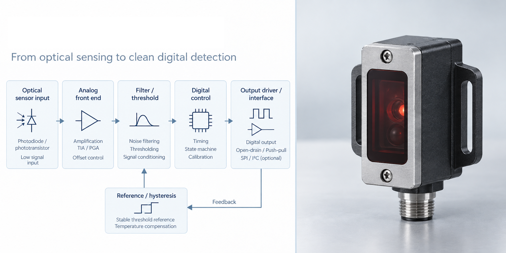
A sensor interface may combine amplification, filtering, threshold detection, simple conversion and digital processing on one die.
Useful for industrial sensors, instrumentation modules and embedded sensing systems.
Custom control IC
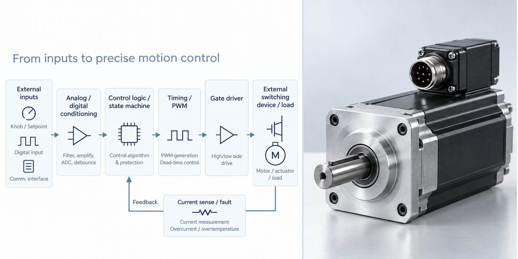
State machines, timing, digital logic and mixed-signal monitoring can replace combinations of small controllers, glue logic and discrete components.
Useful for specialized embedded control.
Board management IC
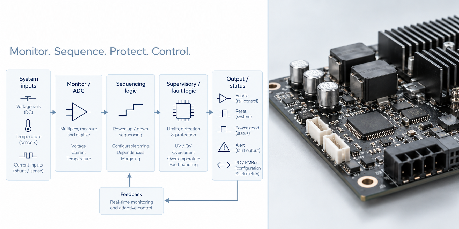
Monitoring, sequencing and supervisory functions rarely require advanced nodes but can benefit significantly from application-specific integration.
Useful for industrial systems, infrastructure electronics and data-center hardware.
Protocol and glue IC
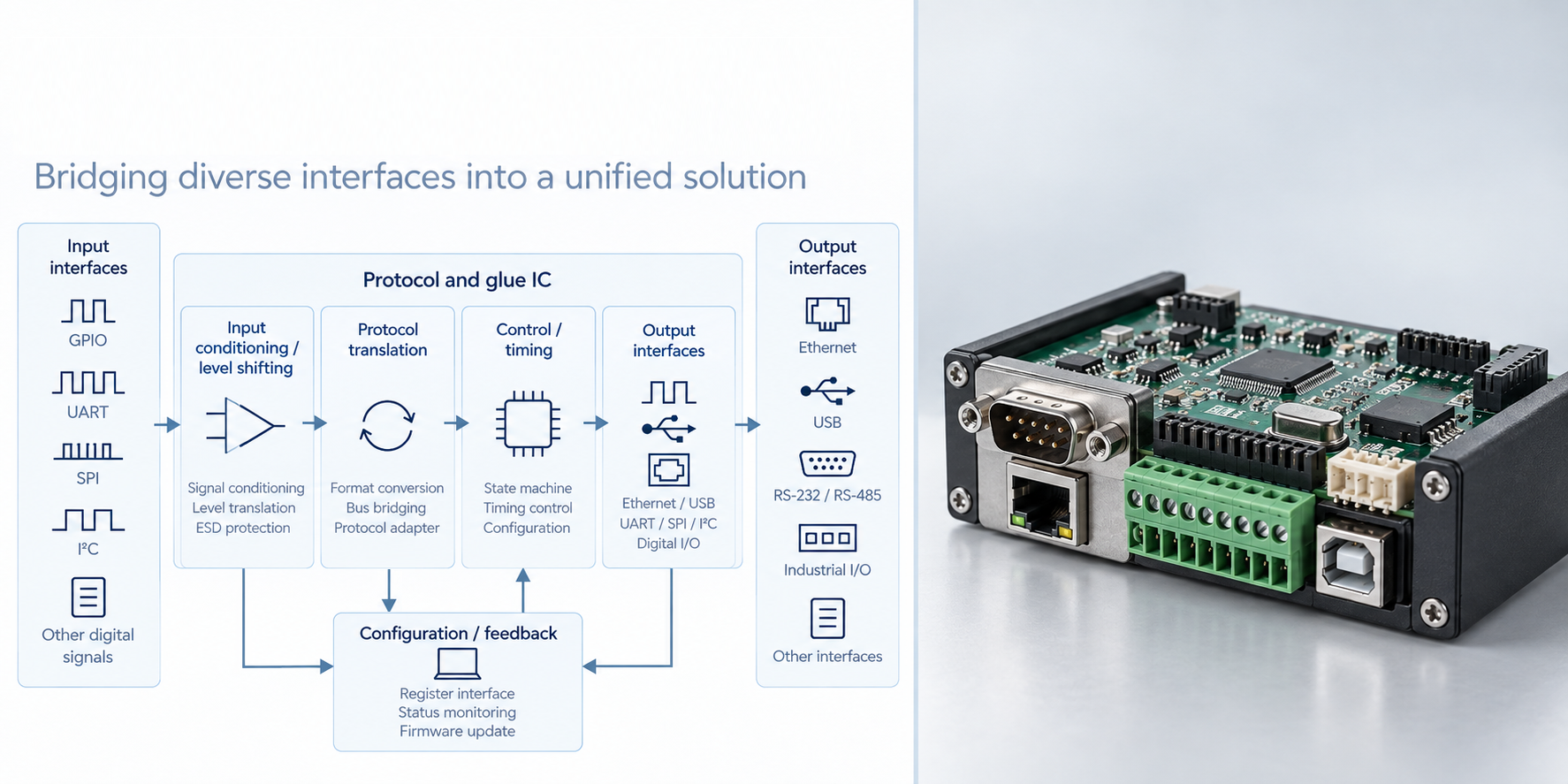
A custom interface chip can absorb product-specific logic that would otherwise be spread across discrete devices, programmable logic and firmware.
Useful where the electronics are unique but volumes do not justify a conventional ASIC programme.
Where Rapid CMOS is not the target
Rapid CMOS is deliberately not designed for every semiconductor application.
Specialized semiconductor processes remain the correct solution for those applications.
It is not intended for
It is not intended for:
Manufacturing platform
A different cost structure for manufacturing.
Advanced semiconductor equipment is economically justified by enormous wafer volumes and valuable silicon.
xSilica starts from a different requirement:
Manufacture small quantities quickly and economically.
By constraining the process, xSilica can also constrain the equipment required to manufacture it.
Purpose-built process modules focus on the capabilities Rapid CMOS actually requires rather than inheriting the rigidity and complexity of general-purpose semiconductor equipment.
That reduces both equipment cost and infrastructure requirements.
Lower capital expenditure matters because manufacturing economics ultimately determine how quickly a fab can afford to start your wafer.
A high-capex fab has to aggregate work and optimize utilization.
A lower-capex manufacturing cell can economically operate with much smaller batches.
That is a direct enabler of rapid silicon iteration.
Equipment developed around the process.
xSilica develops manufacturing equipment alongside the semiconductor process itself. The manufacturing architecture is built from process modules specifically designed around the requirements of Rapid CMOS.
Automation is designed into those modules rather than added to conventional manual semiconductor equipment afterwards. The objective is deterministic execution with minimal operator-dependent variation.
As the platform matures, those process modules are integrated into compact manufacturing cells. Each cell becomes a unit of semiconductor manufacturing capacity that can be replicated rather than enlarged indefinitely.
Integrated characterization and test
Measurement built into the platform.
Rapid manufacturing only creates value if useful measurement follows quickly. xSilica places test structures in the scribe lines for process validation, and develops characterization and test as part of the same platform.
Scribe lines are the sawing margins between dies, lost when the wafer is cut. They leave roughly 100 µm of usable width along two sides of each die: limited, but enough for small structures that can be probed before dicing to characterize that specific wafer.
Designers will ultimately be able to place their own structures in that space. Transistor gain, doping profiles, capacitor values and poly sheet resistance can be measured next to the design itself, without spending a bond pad on the die.
xSilica guarantees the manufacturing process flow, circuit function and the correctness of the supplied stimuli remain the responsibility of the customer. Electrical stimuli and expected measurements are uploaded together with the scribe-line patterns.
Functional test at die level is also available. The die pads are probed directly with customer-supplied stimuli and the results are returned digitally. Because a die can carry more pads than the final package bonds, the number of probing locations is not limited by the pin count of the part. The customer sets the pass criteria, and determines whether only passing dies continue to back-end processing or all dies continue with the measurements returned for information.
Examples include:
The long-term workflow is continuous
The output of a manufacturing run should ultimately be more than physical silicon.
It should also include structured information about what that silicon actually did.
From wafer to usable silicon
Several backend options to match your learning goals.
The default output of Rapid CMOS is bare silicon die. For prototype development, this often gives the shortest path between wafer fabrication and electrical evaluation.
Additional backend capabilities can be added where the application requires them.
Backend flow, packaging options:
Dicing
Individual dies separated and prepared for handling.
Bare die
Fastest path to probing, laboratory fixtures and experimental integration.
Evaluation carriers
Temporary or reusable carriers providing convenient electrical access without requiring a final production package.
Conventional packages
QFN and other formats can be introduced as qualified backend options.
Packaging adds another engineering and logistics cycle. xSilica therefore treats packaging as a configurable backend choice rather than assuming every prototype needs to look like a production component.
Knowledge Bare die, QFN or WLCSP?Continuous Integration
Every wafer improves the platform.
Traditional semiconductor technologies are often described through major process generations. xSilica is also designed to improve continuously within a process generation.
Every wafer produces information about:
Those results feed back into the same platform.
Process
Manufacturing data improves recipe stability and process windows by showing what happens on real wafers. Each run gives the process team evidence to make the next run more predictable.
Models
Measured devices improve electrical simulation by replacing assumptions with data from silicon that has been built. Better models guide the next design with confidence.
Components
Characterization shows how reusable functional blocks perform across process, temperature and supply variation. This gives new projects a stronger foundation.
Design
Better models and process knowledge help engineers make choices the platform can reliably manufacture. This means fewer surprises on the path to working silicon.
Test
More automated measurement returns structured results after each run. Teams can compare expected and observed behaviour, identify what changed and choose the next experiment.
Equipment
Process observations expose where equipment affects repeatability. Those insights improve recipes, tools and procedures across each manufacturing cell.
The node does not need to change for the platform to become substantially more capable.
The same technology becomes more useful every time it runs.
One constrained platform.
Easier design.
Shorter iteration cycles.
Lower commitment per experiment.